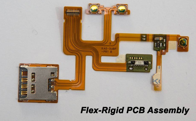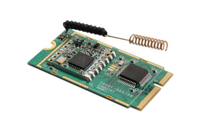

In SkyGlory, Standard PCB service refers to full feature printed circuit board manufacturing service. With 15+ years' experience in PCB fabrication, we have handled hundreds of thousands of PCB projects, and covered almost all kinds of substrate materials including FR4, Aluminum, Rogers, etc. This page only touches standard FR4 based PCB. For PCBs with special technical substrate, please refer to corresponding webpages for information.
Advantages to Standard PCB With LingtechPCB: LingtechPCB everything from prototype to fabrication to assembly. We have been fabricating high quality standard PCB for over ten years and are fully compliant with ISO9001:2008 quality standards. All of our standard PCBs are IPC2 compliant, and we do strict internal quality assurance testing to ensure the board that arrives at your facility is one you know you can rely on. We offer PCB solutions that fit your budget. You can order just a few prototype boards to test your design, and then place a bulk order for your standard PCBs to save even more money. We’ll give you a free instant quote so you’ll know just want to expect and so that you can plan accordingly. We also offer complete technical support from PCB experts. Call us up, chat online or email us with any questions, whichever is the most convenient for you. We’ll handle your concerns or questions as quickly as possible. We have obtained over 99% customer satisfaction rate, and as soon as you start ordering printed circuit boards from LingtechPCB, you’ll find out why.
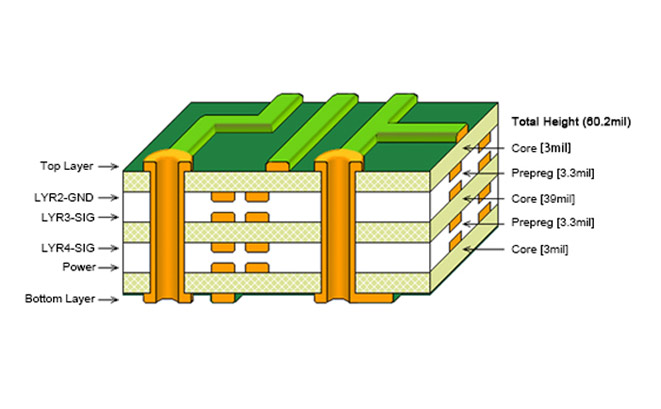
| No. | Item-Double/Multi Layers | Description | Data and Model | ||||
| 1 | Layer | Layer | 1-70 | ||||
| 2 | Material | Brand | SY、ITEQ、KB、NOUYA | ||||
| 3 | Surface treatment | HASL lead-free,Immersion Gold、OSP、Immersion Tin、Immersion Silver、 | |||||
| Plating Gold、Plating Tin、ENEPIG | |||||||
| 4 | Selectivity surface treatment | ENIG+OSP、ENIG+G/F、Flash Gold+G/F、Immersion Silver+G/F、Immersion | |||||
| Tin+G/F | |||||||
| 5 | Solder mask color | green.yellow.black.matte black.blue.red.white.matte green | |||||
| 6 | Silkscreen color | White,yellow,black | |||||
| 7 | Max board size with 2L | mm | 2000*500 | ||||
| 8 | Max board size with 4L,6L | mm | 570*850 or 1150*430(Exceeding 570MM shall be reviewed) | ||||
| 9 | Max board size with more than 8L | mm | 570*670 or 980*430(Exceeding 570MM shall be reviewed) | ||||
| 10 | MiN board size | mm | 0.5*1.0mm(thickness≤0.5mm)、1.0*2.0mm(thickness≥0.5mm) | ||||
| 11 | Min outline tolerance | mm | ±0.05mm(Laser Routing) 、±0.1mm(Mechanical Routing) | ||||
| 12 | Board Thickness | mm | 0.13-8mm | ||||
| 13 | Double side board thickness | mm | 0.13-3.6mm | ||||
| 14 | 4Layers board thickness | mm | 0.30-7mm | ||||
| 15 | 6Layers board thickness | mm | 0.6-8mm(6L)、0.8-8mm(8L)、1.0-8mm(10L)、1.0-8mm(12L) | ||||
| 16 | The tolerance of board thickness | mm | ±0.1mm(thickness≤1.0mm)、±10%mm(thickness>1.0mm) | ||||
| 17 | Min Drilling hole size | mm | 0.075-0.1mm(Laser)、0.15mm(Mechanical) | ||||
| 18 | Single Max Drilling | mm | 6.5mm(Drill Bit) | ||||
| 19 | Max Drilling | mm | 50mm | ||||
| 20 | Min PTH tolerance | mm | ±0.05mm、±0.075mm | ||||
| 21 | Min NPTH tolerance | mm | ±0.05mm(Limitation+0、-0.05mm or +0.05、-0mm) | ||||
| 22 | Min hole tolerance | mm | ±0.075mm | ||||
| 23 | Max Drilling tolerance | mm | ±0.1mm | ||||
| 24 | Slot hole | mm | 0.5-6mm | ||||
| 1/8 | |||||||
| 25 | Min slot hole length | mm | 1.0mm | ||||
| 26 | Slot hole aspect ratio | mm | 1:2 | ||||
| 27 | Min slot hole tolerance | mm | Slot width、±0.15mm | ||||
| 28 | Min slot hole tolerance | mm | Slot width direction±0.10、slot length direction±0.15 | ||||
| 29 | Countersink hole angle & size | Big hole82、90、120degree、dia≤10mm | |||||
| 30 | Countersink hole angle & size | PTH & NPTH、Big hole angle 130degree、The dia of the large hole is not | |||||
| greater than 6.3mm | |||||||
| 31 | Min pattern width / spacing | mm | 0.075mm/0.075mm | ||||
| 32 | Pattern width tolerance | mm | ±20um | ||||
| 33 | Min pad | mm | 0.15mm | ||||
| 34 | FR-4 PP | 106、1080、3313、2116、7628 | |||||
| 35 | Mult press blind buried hole production | Press on the same side≤5 | |||||
| 36 | Max bore diameter of pad hole plug hole | mm | 0.4 Multi press blind & buried hole board | ||||
| 37 | Min thickness of inner | mm | 0.05(none blind buried hole)、0.13(blind buried hole) | ||||
| 38 | Min inner | mil | 3(18um base copper)、4(35um base copper)、≥3mil | ||||
| 39 | Inner layer treatment | Brown Oxygen | |||||
| 40 | Min inner pattern spacing(105um base | mil | 5 | ||||
| copper、after compensation) | |||||||
| 41 | Min inner layer pattern spacing(140um base | mil | 7 | ||||
| copper、after compensation) | |||||||
| 42 | Min innner layer pattern spacing(18um base | mil | 3 | ||||
| copper、after compensation) | |||||||
| 43 | Min inner layer pattern spacing(35um base | mil | 3.5 | ||||
| copper、after compensation) | |||||||
| 44 | Min inner layer pattern spacing(70um base | mil | 4 | ||||
| copper、after compensation) | |||||||
| 45 | Min inner layer pattern width(105umbase | mil | 5 | ||||
| copper、before compensation) | |||||||
| 2/8 | |||||||
| 46 | Min inner layer pattern width(140um base | mil | 7 | ||
| copper、before compensation) | |||||
| 47 | Min inner layer pattern width(18um base | mil | 3 | ||
| copper、before compensation) | |||||
| 48 | Min inner layer pattern width(35um base | mil | 3 | ||
| copper、before compensation) | |||||
| 49 | Min inner layer pattern width(70um base | mil | 4 | ||
| copper、before compensation) | |||||
| 50 | Min outer layer pattern spacing(105um | mil | 6 | ||
| base copper、after compensation) | |||||
| 51 | Min outer layer pattern spacing(12、18um | mil | 3.0(18um)、2.5(12um) | ||
| base copper、after compensation) | |||||
| 52 | Min outer layer pattern spacing(140um | mil | 7 | ||
| base copper、after compensation) | |||||
| 53 | Min outer layer pattern spacing(35um base | mil | 3.5 | ||
| copper、after compensation) | |||||
| 54 | Min outer layer pattern spacing (70um base | mil | 5 | ||
| copper、after compensation) | |||||
| 55 | Min outer layer pattern width(105um base | mil | 8 | ||
| copper、before compensation) | |||||
| 56 | Min outer layer pattern width(12、18um | mil | 3.5(18um)、3(12um) | ||
| base copper、before compensation) | |||||
| 57 | Min outer layer pattern width(140um base | mil | 9 | ||
| copper、before compensation) | |||||
| 58 | Min outer layer pattern width(35um base | mil | 4.5 | ||
| copper、before compensation) | |||||
| 59 | Min outer layer pattern width(70um base | mil | 6 | ||
| copper、before compensation) | |||||
| 3/8 | |||||
| 60 | Min.spacing from pattern to pad, pad to pad | mil | 3(12、18um)、3.5(35um)、5(70um)、6(105、140um) | |||
| for outer layer(after compensation) | ||||||
| Min.outer pattern and spacing with | ||||||
| 61 | blind/buried holes plated many times(>=2 | mil | 3.5/3.5 (before compensation) | |||
| times) | ||||||
| 62 | Min distance from inner layer edge without | mil | 10 | |||
| copper leakage | ||||||
| 63 | Min inner layer isolation width | mil | 8 | |||
| 64 | Min inner layer isolation ring | mil | 8(≤6layer)、10(≥8layer) | |||
| 65 | Min single side width of inner pad(none | mil | 4.5(18、35um、Can be partial 4)、6(70um)、8(105um) | |||
| blind buried hole) | ||||||
| 66 | Min single side width of inner pad(laser | mil | 3 | |||
| hole) | ||||||
| 67 | Impedance tolerance | % | ±5Ω(<50Ω)、±10%(≥50Ω);≥50Ω 可±5% | (need to | ||
| evaluate when it requests)、 | ||||||
| 68 | Min BGA pad diameter | mil | 7mil | |||
| 69 | Min pad diameter | mil | 12(0.10mmMechanical or laser drilling) | |||
| 70 | Min hole copper thinckness(none blind | um | average 25、min single point≥20 | |||
| buried hole) | ||||||
| 71 | Min hole copper thinckness(blind buried hle | um | averager 20、min single point≥18 | |||
| ) | ||||||
| 72 | PP thickness(min) | um | 0.075(only H oz base copper) | |||
| 73 | ENIG: gold thickness | um | 0.025-0.10 | |||
| 74 | ENIG; nickle thickness | um | 3-5 | |||
| 75 | Immersion silver.silver thickness | um | 0.1-0.3 | |||
| 76 | Min HASL LeadFree/pure tin thickness | um | 0.4 | |||
| 77 | Gold Finger:gold thickness | um | 0.25-1.3(The required value is the thinnest point) | |||
| 4/8 | ||||||
| 78 | Gold Finger:nickle thickness | um | 3-5 | |||
| 79 | Flash Gold: gold thickness | um | 0.025-0.10 | |||
| 80 | Golden finger chamfer Angle tolerance | ±5° | ||||
| 81 | Golden finger chamfering margin tolerance | mil | ±5 | |||
| 82 | Min gold finger length | inch | 2 | |||
| 83 | Min distance between gold fingers | mil | 6 | |||
| 84 | Gold finger next to the TAB does not hurt | mm | 7(Means automatic chamfering) | |||
| the min distance | ||||||
| 85 | Long and short gold finger | Can be combined with various surface treatments | ||||
| 86 | Surface treatment for long and short gold | Immersion gold;Flash gold | ||||
| finger | ||||||
| 87 | Immersion tin:Tin thickness | um | 0.8-1.5 | |||
| 88 | Electroplate hard gold thick | um | 0.15-1.3 | |||
| 89 | Flash Gold: nickle thickness | um | 3-5 | |||
| 90 | Max borad thickness of mechanical drilling | mm | 0.60 | |||
| 0.10mm | ||||||
| 91 | Max borad thickness of mechanical drilling | mm | 1.20 | |||
| 0.15mm | ||||||
| 92 | Max borad thickness of router bit 0.25mm | mm | 5 | |||
| 93 | Bow and twist capability limit | % | 0.1(need to evaluate when it requests ≤0.3) | |||
| 94 | Max Dry film sealing slot | 5mm*3.0mm;More than one side of sealing hole15mil | ||||
| 95 | Min unilateral width of dry film sealing hole | mil | 10 | |||
| 96 | Max diameter of dry film sealing hole | mm | 4.5 | |||
| 97 | Min width of solder mask opening | mil | 8 | |||
| 98 | Min solder mask thickness | um | 10 | |||
| 99 | Min S/M bridge width | mil | 3(green)、5(other color)(base copper≤1OZ)(base coppe2-4OZ、All in | |||
| accordance with the 6mil) | ||||||
| 5/8 | ||||||
| 100 Min unilateral width of solder mask | mil | 2.5(Allow local2mil) | |||||
| 101 Min solder mask opening (sing side) | mil | 2(Flash gold local 1.5、other allow local 1) | |||||
| 102 Max diameter of ink plug hole(both side) | mm | 0.65 | |||||
| 103 Thickness of solder mask ink through hole | um | 5/8 | |||||
| cover | |||||||
| 104 V-CUT Angle specifications | 20°、30°、45°、60° | ||||||
| 105 V-CUT(1.0<H≤1.6mm) | mm | 0.36(20°)、0.4(30°)、0.5(45°)、0.6(60°) | |||||
| 106 V-CUT(1.6<H≤2.4mm) | mm | 0.42(20°)、0.51(30°)、0.64(45°)、0.8(60°) | |||||
| 107 V-CUT(2.5≤H≤3.0mm) | mm | 0.47(20°)、0.59(30°)、0.77(45°)、0.97(60°) | |||||
| 108 V-CUT(H≤1.0mm) | mm | 0.3(20°)、0.33(30°)、0.37(45°)、0.42(60°) | |||||
| 109 V-CUT Symmetry tolerance | mil | ±4 | |||||
| 110 V-CUT Angle tolerance | o | ±5° | |||||
| 111 V-CUT Residue thickness | mil | ±4 | |||||
| 112 Blue glue white mesh plug hole max | mm | 2 | |||||
| diameter | |||||||
| 113 Min single side of blue cover pattern or pad | mil | 2 | |||||
| 114 Max diameter of blue plastic aluminum plug | mm | 4.5 | |||||
| hole | |||||||
| 115 Min isolation between blue glue and pad | mil | 12 | |||||
| 116 Min single side carbon cap pattern | mil | 2 | |||||
| 117 Min isolation between carbon and pad | mil | 8 | |||||
| 118 Min isolation between carbon and carbon | mil | 12 | |||||
| 119 Min gridding spacing | mil | 5(12、18、35 um)、8(70 um) | |||||
| 120 Min gridding width | mil | 5(12、18、35 um)、10(70 um) | |||||
| 121 Min silk width and height(12、18um base | width4mil;height:23mil | ||||||
| copper) | |||||||
| 122 Min silk width and height(35um base | width5mil;height:30mil | ||||||
| copper) | |||||||
| 6/8 | |||||||
| 123 Min silk width and height(70um base | width 6mil;height:45mil | |||
| copper) | ||||
| 124 | Min isolation of silk and pad | mil | 6 | |
| 125 Min test on resistance | Ω | 10 | ||
| 126 | Min distance from test point to edge | mm | 0.5 | |
| 127 Max test current | mA | 200 | ||
| 128 Max test voltage | V | 250 | ||
| 129 WNH | mil | 3.9 | ||
| 130 Min test pad | mil | 3.9 | ||
| 131 Min etch logo width | mil | 8(12、18um)、10(35um)、12(70um) | ||
| 132 | Outline tolerance(edge to edge) | mil | ±4(Complex outlin and inner grooves with this requirement shall be reviewed) | |
| 133 | Min inner angular radius | mm | 0.4 | |
| 134 | Depth control slot hole(edge)or Blind slot | mm | ±0.10 | |
| precision(NPTH) | ||||
| Special tolerance requirements for board | ||||
| 135 thickness(No interlayer structure | mm | ≤2.0±0.1;2.0-3.0±0.15;≥3.0±0.2 | ||
| requirement) | ||||
| 136 | Max ratio of plate thickness to hole | 20:1(not inclue≤0.2mm diameter、more than 12:1 shall be reviewed)) | ||
| 137 Min hole diameter | mm | 0.45 | ||
| 138 Outline method | Routing,V-CUT,Stamp-hole | |||
| 139 | Min router bit diameter of outline | mm | 0.6 | |
| 140 | Min. distance from hole to trace(Not | mil | 6(≤8layers)、8(≤14layers)、9(≤28layers) | |
| blind/buried holes) | ||||
| 141 | Min. distance from hole to trace (blind / | mil | 9(Press one time);10(press two times or three times) | |
| buried holes) | ||||
| 142 | Min distance from hole to trace(Laser drill, 1 | mil | 6 | |
| or 2-step) | ||||
| 7/8 | ||||
| 143 Min single-sided width for via hole pad of | mil | 4(12、18um)3.5、4.5(35um)、6(70um)、8(105um)、10(140um) | |
| outer layer | |||
| 144 Min. distance without copper exposure | mil | 8 | |
| when outline routing | |||
| 145 Maximum insulation resistance(for test) | MΩ | 100 | |
| 146 Hole resistance test board thickness limit | mm | 0.38-5.0 | |
| 147 Hole resistance test aperture limit | mm | min:0.62mm、max0.25mm | |
| 148 ionic soil | ug/cm2 | ≤1 | |
| 149 Copper stripping strength | N/cm | 7.8 | |
| 150 Resistance weld hardness | H | 6 | |
| 151 Resistance | 94V-0 | ||
| 152 RCC material | um | copper foil:12,resin:65,100um(complete55、90um) | |
| 153 Thkickness of blue glue | mm | 0.2-0.5 | |
| 154 Min carbon pattern width | mm | 0.5mm | |
| 155 | Hole resistance test aperture limit | ||