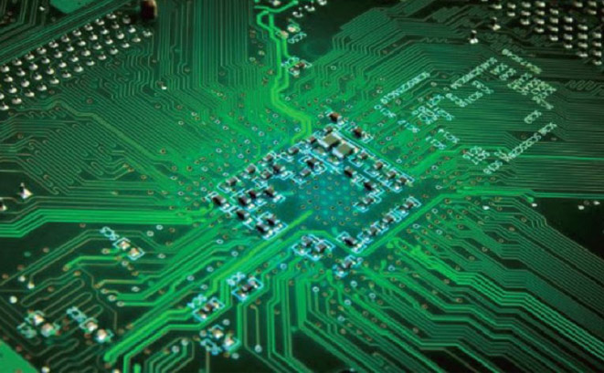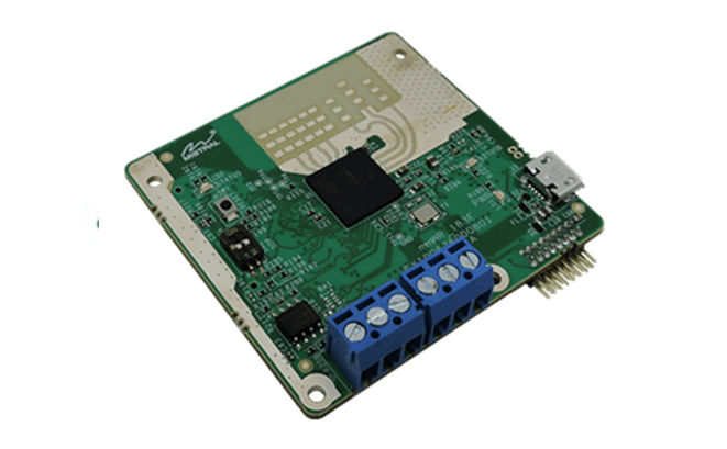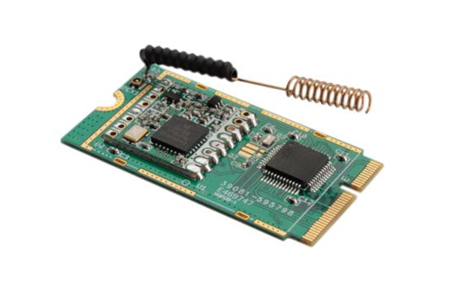
Blind Vias Backplane PCB
BackplanePCB usually used a Printed Circuit Board also have been used in minicomputers and high reliability
applications.To be a group of electrical connector in parallel with each others, each pin in PCB to each connectors
are linked to the same relative pins of all the other connectors forming a internal systems.That is used as a
backbone to connect several PCBs together to make up a complete system.
BackplanePCB is often described as being either active or passive. Active backplanes contain, in addition to the
sockets, logical circuitry that performs computing functions. In contrast, passive backplanes contain almost no
computing circuitry.Traditionally, most PCs have used active backplanes PCB. also including Consumer Electronics
PCB, Indeed, the terms motherboard and backplane have been synonymous. Recently, though, there has been a
move toward passive backplanes, with the active components such as the CPU inserted on an additional card.
Passive backplanes make it easier to repair faulty components and to upgrade to new components.
HCH-PCB service our customers from prototype through mass production in Backplanes PCB, meeting their lead
time to market requirements. No order is too small. We thrive in a high mix, quick turn environment.
Our on-time delivery, for standard as well as complex technology is in the 97% across all industries.
Bling Vias Backplane PCB Capability:
| Appearance | Standard | High | Advanved |
| Layer Count (Max.Layers): | 16 | 40 | 60+ |
| PCB Size (Max.): | 1100mm×500mm | 1200mm×500mm | 1200mm×630mm |
| Thickness (Max.): | 8mm | 10mm | 15mm+ |
| Outer Layer Line Width/Space: | 0.006〞/0.006〞 | 0.005〞/0.005〞 | 0.004〞/0.004〞 |
| Press-fit Hole Size Tolerance | +/-2mil | +/-2mil | +2/-1mil |
| Through Hole Aspect Ratio: | 15:1 | 17:1 | 20:1 |
| Drill Registration: | +/-5mil | +/-4mil | +/-3mil |
| Buried Vias: | Yes | Yes | Yes |
| Blind Vias: | Layers n to n-1 | Layers n to n-2 | Layers n to n-3 |
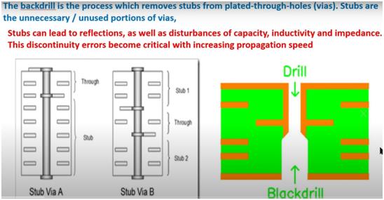
Back Drilling (Counter Bore):
Backplanes boards can endure significant signal integrity disturbances as a result of the unused portions of
through holes and vias that extend past their last connected layer. known as “stubs”. it will lead SI reflections,
capacitance, inductance and impedance discontiunities,losses that become critical as speeds increase.