LingtechPCB have top-level equipment and advanced process technology, no matter how complex the PCB,
LingtechPCB can quickly provide manufacturing services according to customer requirements.
And has a senior engineering technical team,
according to the customer’s design to make fabrication in a low-cost manner
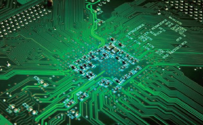
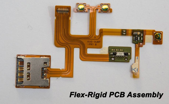
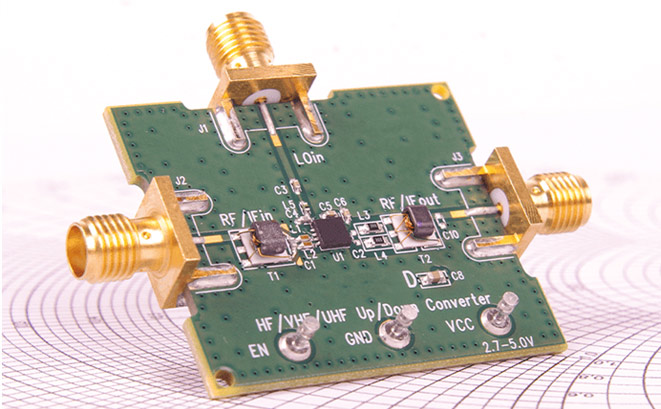
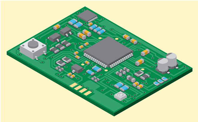
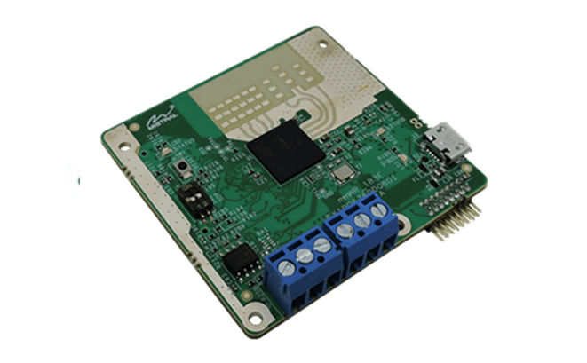
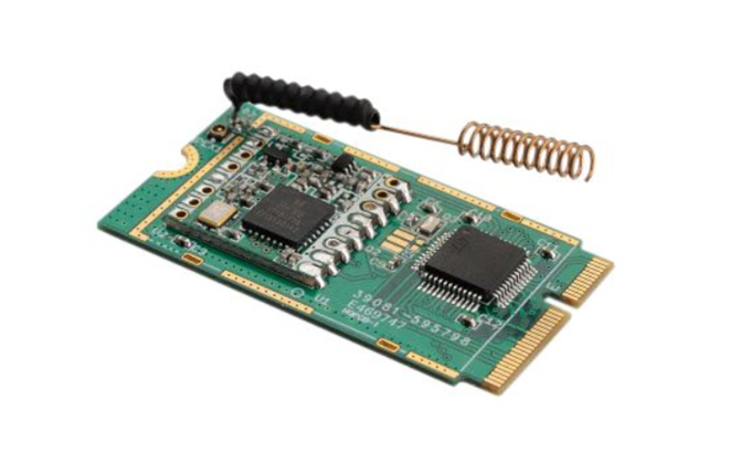
LingtechPCB offers top quality Printing Circuit Boards (PCB) including multi-layer PCB (printed circuit board),
high-level HDI(high density inter-connector), arbitrary-layer PCB and rigid-flexible PCB…etc.
As a base material, LingtechPCB understands the importance of reliable quality of the PCB.
We invest in best equipments and talented team to produce best quality boards.
LingtechPCB manufacturing capabilities are shown in the chart below.
|
Type |
Capability |
|
Scope |
Multilayers(4-70)、HDI(4-48)Flex、Rigid Flex |
|
Double Side |
CEM-3、 FR-4、Rogers RO4233、Bergquist Thermal Clad 4mil–126mil (0.1mm-3.2mm) |
|
Multilayers |
4-70 layers, board thickness 8mil-126mil (0.2mm-3.2mm) |
|
Buried/Blind Via |
4-48 layers, board thickness 10mil-126mil(0.25mm-3.2mm) |
|
HDI |
1+N+1、2+N+2、3+N+3、Any layer |
|
Flex & Rigid-Flex PCB |
1-8layers Flex PCB ,2-12layers Rigid-flex PCB HDI+Rigid-flex PCB |
|
Laminate |
|
|
Soldermask Type(LPI) |
Taiyo、Goo’s、Probimer FPC….. |
|
Peelable Soldermask |
|
|
Carbon ink |
|
|
HASL/Lead Free HASL |
Thickness: 0.5-40um |
|
OSP |
|
|
ENIG (Ni-Au) |
|
|
Electro-bondable Ni-Au |
|
|
Electro-nickel palladium Ni-Au |
Au: 0.015-0.075um Pd 0.02-0.075um Ni:2-6umm |
|
Electro. Hard Gold |
|
|
Thick tin |
|
|
Capability |
Mass Production |
|
Min Mechanical Drill Hole |
0.20mm |
|
Min. Laser Drill Hole |
4mil (0.100mm) |
|
Line Width/Spacing |
2mil/2mil |
|
Max. Panel Size |
21.5″ X 24.5″(546mm X 622mm) |
|
Line Width/Spacing Tolerance |
Non electro coating:+/-5um,Electro coating:+/-10um |
|
PTH Hole Tolerance |
+/-0.002inch(0.050mm) |
|
NPTH Hole Tolerance |
+/-0.002inch(0.050mm) |
|
Hole Location Tolerance |
+/-0.002inch(0.050mm) |
|
Hole to Edge Tolerance |
+/-0.004inch(0.100mm) |
|
Edge to Edge Tolerance |
+/-0.004inch(0.100mm) |
|
Layer to Layer Tolerance |
+/-0.003inch(0.075mm) |
|
Impedance Tolerance |
+/- 10% |
|
Warpage % |
Max≤0.5% |
Technology for HDI PCB
|
ITEM |
Production |
|
Laser Via Drill/Pad |
0.125/0.30 、 0.125/0.38 |
|
Blind Via Drill/Pad |
0.25/0.50 |
|
Line Width/Spacing |
0.10/0.10 |
|
Hole Formation |
CO2 Laser Direct Drill |
|
Build Up Material |
FR4 LDP(LDD); RCC 50 ~100 micron |
|
Cu Thickness on Hole Wall |
Blind Hole: 10um(min) |
|
Aspect Ratio |
0.8 : 1 |
Technology for Flexible PCB
|
Project |
Ability |
|
Roll to roll (one side) |
YES |
|
Roll to roll (double) |
NO |
|
Volume to roll material width mm |
250 |
|
Minimum production size mm |
250×250 |
|
Maximum production size mm |
500×500 |
|
SMT Assembly patch (Yes/No) |
YES |
|
Air Gap capability (Yes/No) |
YES |
|
Production of hard and soft binding plate(Yes/No) |
YES |
|
Max layers(Hard) |
10 |
|
Tallest layer(Soft plate) |
6 |
|
Material Science |
|
|
PI |
YES |
|
PET |
YES |
|
Electrolytic copper |
YES |
|
Rolled Anneal Copper Foil |
YES |
|
PI |
|
|
Covering film alignment tolerance mm |
±0.1 |
|
Minimum covering film mm |
0.175 |
|
Reinforcement |
|
|
PI |
YES |
|
FR-4 |
YES |
|
SUS |
YES |
|
EMI SHIELDING |
|
|
Silver Ink |
YES |
|
Silver Film |
YES |