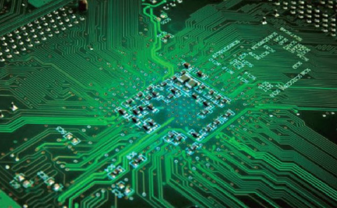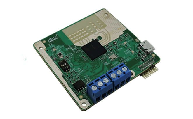
After placing the placement machine components and performing quality control, the next step is to move the circuit
board to DIP production to complete the assembly of the through-hole components.
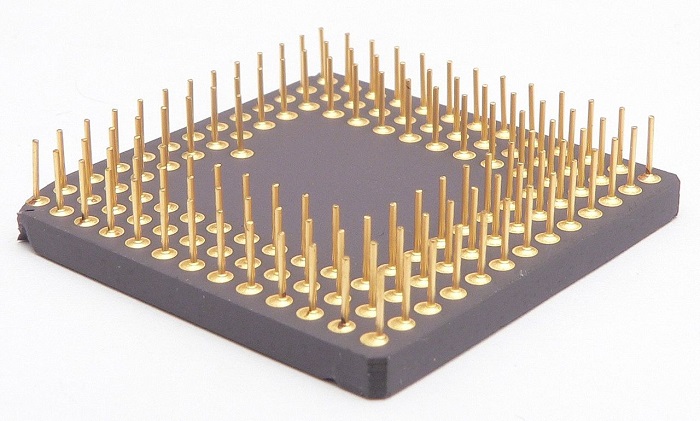
Dual in-line packaging is called DIP, which is a method of packaging integrated circuits. The shape of the integrated
circuit is rectangular, and there are two rows of parallel metal pins on both sides of the IC, which are called pin
headers.
DIP packaged components can be soldered in the plated through holes of the printed circuit board or inserted into
the DIP socket.
1.DIP function:
The chip using this packaging method has two rows of pins, and these pins can be directly soldered on the chip socket with the DIP structure, or soldered in the same number of solder holes. Its characteristic is that it can easily realize the through-hole soldering of the printed circuit board, and it has good compatibility with the main board.
2.The difference between placement machine and DIP
Mounters usually install lead-free or short-lead surface mount components. The solder paste needs to be printed on the circuit
board, and then installed by the chip mounter, and then the device is fixed by reflow soldering.
DIP soldering is a directly packaged device, which can be fixed by wave soldering or manual soldering.